Image of a heterotube diode:
Sushi-Like Rolled 2D Heterostructures May Lead To New Miniaturized Electronics
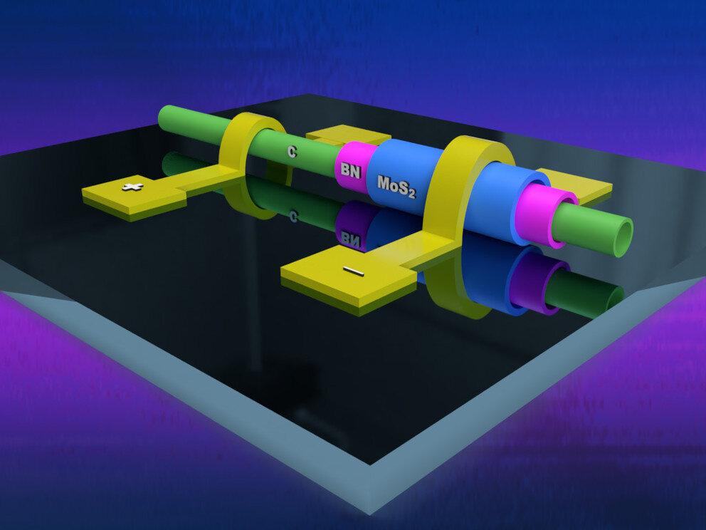
Jamie Oberdick, Pennsylvania State University | Phys.org | 3/10/21This device contains a MoS2 semiconductor shell (blue), over the insulator hBN shell (purple), over the carbon nanotube core (green) of the heteronanotube covered with gold electrodes (yellow). Credit: Elizabeth Flores-Gomez Murray/ Penn State.
Next step: getting it to stop making that “Pew! Pew! Pew!” sound.
It could go, “Pepe Pepe Pepe”.
“Do we really need to keep painting them fluorescent colors?”
“YES! That is the most important part!”
I used to know some of that stuff. Source?
Rabbit meet hole.
https://www.researchgate.net/publication/344393106_MXenes-Based_Bioanalytical_Sensors_Design_Characterization_and_Applications
Wanted to know why Mos2…
Ohh I see. They are made in three simple steps:
The wet chemical route is based on three simplesteps: (1) Etching, (2) delamination, and (3) intercalation. Due to the use of HF as an etchant,MXene layers are primarily terminated with F and OH/=O functional groups, abbreviated as Txtogive a general formula of Mn+1XnTx,n=1–3. The etching is simply done by immersing the MAXphase in HF. Alhabeb et al. studied the effect of different concentrations of HF on the morphologyof the resulting MXene. The results of the study have shown that Al can be etched by usingHF concentration as low as five weight percent; however, for low HF concentrations, the MXenedid show the characteristic accordion-like morphology that was observed in the case of 30% HF.After completing the etching process, the powder was washed thoroughly with deionized water bysuccessive centrifugation cycles at 3500 rpm. After each cycle, the supernatant was decanted andreplaced with fresh deionized water. The washing process continued until the pH of the supernatanthas reached 6 to 7. Delamination is the second crucial step in the synthesis protocol that enhances theaccessible surface area of the nanomaterial. In order to delaminate MXene nanosheets, the van der Waalsforces between the adjacent MX sheets have to be broken. This barrier is relatively strong for MXenes(with their ~2.2 Å interlayer distance) compared to that of graphene (3.35 Å). A well-established methodfor the delamination of MXenes is to increase the interlayer distance through intercalation, achieved byinserting external elements (ions or molecules) in between the layers of the laminated material.Large, organic molecules, such as dimethyl sulfoxide (DMSO), isopropylamine, tetraalkylammoniumhydroxides (TBAOH), were some of the first intercalants used for expanding the interlayer spacing ofTi3C2Tx MXenes synthesized with HF [4]. Figure 1shows a general synthesis scheme for producingMXenes (left) and examples of SEM micrographs (right) displaying the ‘accordion’-like morphologythat is typical of various MXenes compositions. For description of detailed synthesis methodologies,readers are referred to other literature, specifically discussing the synthesis protocol of MXenes [5,6]
Simple, like I said.
Thanks, Fangbeer; it’s been soooo long; and I was never into semi-conductors that much. I just wanted to know what h-BN was; turns out it’s hexagonal boron nitride. Nutty semiconductor people will take anything and try to make a semi-conductor out of it (just cause silicon carbide took off from being an abrasive to a semi-conductor in the ’80 they gotta try everything, but the sushi roll/hot dog thing is a neat trick.
I might would have parsed that better if I were awake. I might try again tomorrow.
Seems like their interest in things like h-BN and Mos2 is their biological compatibility. They’re trying to build nanobots to invade your body…
Weird. Transistors and diodes are currently made by layering materials and laser etching.
That seems like it would be harder to manufacture, though from a little research I can’t quite tell if these are printed in a similar way to what we do now and subsequently rolled, or chemically “grown” like that.